
Notes on AI Hardware
Usually, I write about the Algorithms behind AI, but once in a while, it’s okay to visit the hardware side as well. All these algorithmic advances would never have been realized if not for the crazy innovation on the hardware side as well. Nvidia and all other chip manufacturing companies are growing at a crazy fast speed, and as a result, they almost doubled or tripled their worth in a single year. But this is not a finance blog, so we are going to keep our focus on AI-related hardware, especially the GPU. In today's blog, we are going to dive super deep into AI hardware architecture.
Table of Contents:
- Difference between CPU, GPU, and TPU
- Why Compute is so Important for AI?
- Overview of the H100
- Breakdown of the Chip
Are you looking for AI content that’s both original and insightful instead of repetitive and copy-pasted content? Want to delve deeper into the technological aspects rather than skimming through surface-level tips and tricks? Discover the AIGuys Digest Newsletter.
And if you want to up your AI game, please check my new book on AI, which covers a lot of AI optimizations and hands-on code:
Difference between CPU, GPU, and TPU
Let’s take a quick look at these three.
CPUs
CPUs are general-purpose computing devices or processors that can handle a complex range of tasks. CPUs typically have fewer cores ranging from anywhere between 2 to 32 with quite a bit of clock speed. Each core is capable of executing a series of instructions serially, making CPUs excellent for tasks that require complex decision-making, branching, or data dependency resolution. All of us already know about the use cases of a CPU, so I’m not going to talk about that.
But let’s talk about Branch Prediction, Out-of-Order Execution, and Speculative Execution.
Branch prediction is a feature in modern CPUs designed to improve performance by guessing the outcome of conditional operations, such as if-then-else statements, before they are actually evaluated. The CPU looks at the history of similar past operations to predict whether a conditional branch will be taken or not. If the prediction is correct, the CPU can continue executing subsequent instructions without interruption, significantly reducing wasted cycles that would occur from waiting for the branch to be resolved. This process helps maintain a steady flow of instruction execution, enhancing overall processing speed.
Out-of-order execution allows a CPU to execute instructions as soon as their input dependencies are met, rather than adhering to their original sequence in the program. This is achieved by fetching and decoding instructions in order, then executing them out of order when all necessary resources are available, and finally committing the results in the original order to preserve the logical flow of the program. This technique improves the efficiency of the CPU’s instruction pipeline, reducing idle times by filling execution gaps caused by delays, such as waiting for data to be fetched from memory.
Speculative execution is an extension of out-of-order execution, where the CPU not only executes instructions out of their original order but also processes instructions that may not ultimately be needed. Based on the outcome of branch prediction, the CPU preemptively executes instructions ahead of a branch before knowing whether those instructions are required according to the program’s flow. If the prediction is correct, the speculative execution results are retained, providing a significant speed boost. If incorrect, the speculative results are discarded, and the correct path is executed, ensuring program accuracy. This process aims to maximize CPU efficiency by reducing idle time, although it has raised security concerns due to the potential exposure of sensitive data through speculative execution paths.
GPUs
GPUs are simple processors, containing thousands of cores, primarily designed for parallel execution. Initially developed for rendering graphics and video processing, their architecture makes them exceptionally good at matrix and vector computations. This parallelism allows them to perform many operations simultaneously, significantly speeding up rendering and scientific computations.
Don’t worry, we’ll look into great detail about GPU architecture in the next sections.
TPUs
TPUs are basically custom Application Specific Integrated Circuits or ASICs. TPUs were invented by Google to accelerate machine learning and AI-related workloads. They are optimized for high throughput of low-precision arithmetic (e.g., 8-bit integers or floating-point operations), and their architecture is tailored for tensor operations, which are fundamental in neural network computations. TPUs are designed to speed up specific types of computations common in neural networks, like matrix multiplications and convolutions.
CPUs are general-purpose processors suitable for a wide range of tasks, GPUs are specialized for parallel processing, and TPUs are even more specialized for machine learning tasks.
CPUs have fewer, more powerful cores designed for sequential processing. GPUs have thousands of simpler cores for parallel tasks. TPUs have specialized circuitry designed explicitly for high-speed tensor operations.
CPUs support a wide range of data types and operations with high precision, making them versatile. GPUs balance between precision and parallel efficiency, suitable for graphics and computation. TPUs often use lower precision arithmetic, optimizing for the specific requirements of machine learning computations, offering significant speedups and efficiency in their domain.
Why compute is so Important for AI?
The real reason why suddenly AI has boomed so much is not primarily due to the algorithmic innovations, but it is the amount of computing that has increased in the last few years. It has already beaten the Morse law in GPU space at least. It’s not that we didn’t do anything on the algorithmic side, but all these upscales were possible due to increased computing primarily. The algorithms behind tools like ChatGPT and Gemini have been present with us since 2018, we are still using pretty much the same old architectures. But the amount of computing that we were able to throw at it changed everything.
A few days ago, I tried to fine-tune Llama7b 2 on 3 MB data. It required a 16 GB GPU whopping 5 days to finish just 10 epochs. And this model is at least 10–100 times smaller than what’s out there. The training cost of ChatGPT was around 100 million USD and for Llama 2 it was around 20–30 million USD.
Modern GPU clusters are extremely power-hungry. GPT 4 used around 50 GWh of energy usage during training. To put this in perspective training GPT-4 in Germany is equivalent to 30 average cars circling the globe 300 times. Google states that one search uses 0.28 Wh, compared to Google GPT 4 uses approximately four times more energy than a Google search.
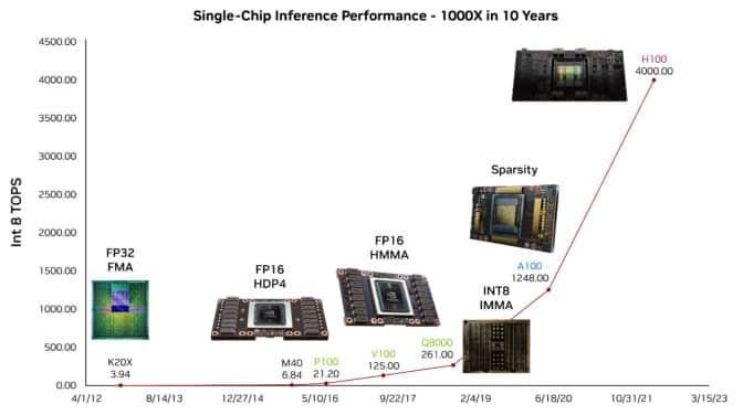
In the last 10 years, the GPU compute increased by a factor of 1000, not a small feat by any means. But we should not forget about the contribution of reduced floating point operation (Quantization: FP16, INT8), this itself helped us increase the capacity to feed our AI algorithms much more data with less resource usage.
Overview of the H100
Let’s analyze what are these different components.
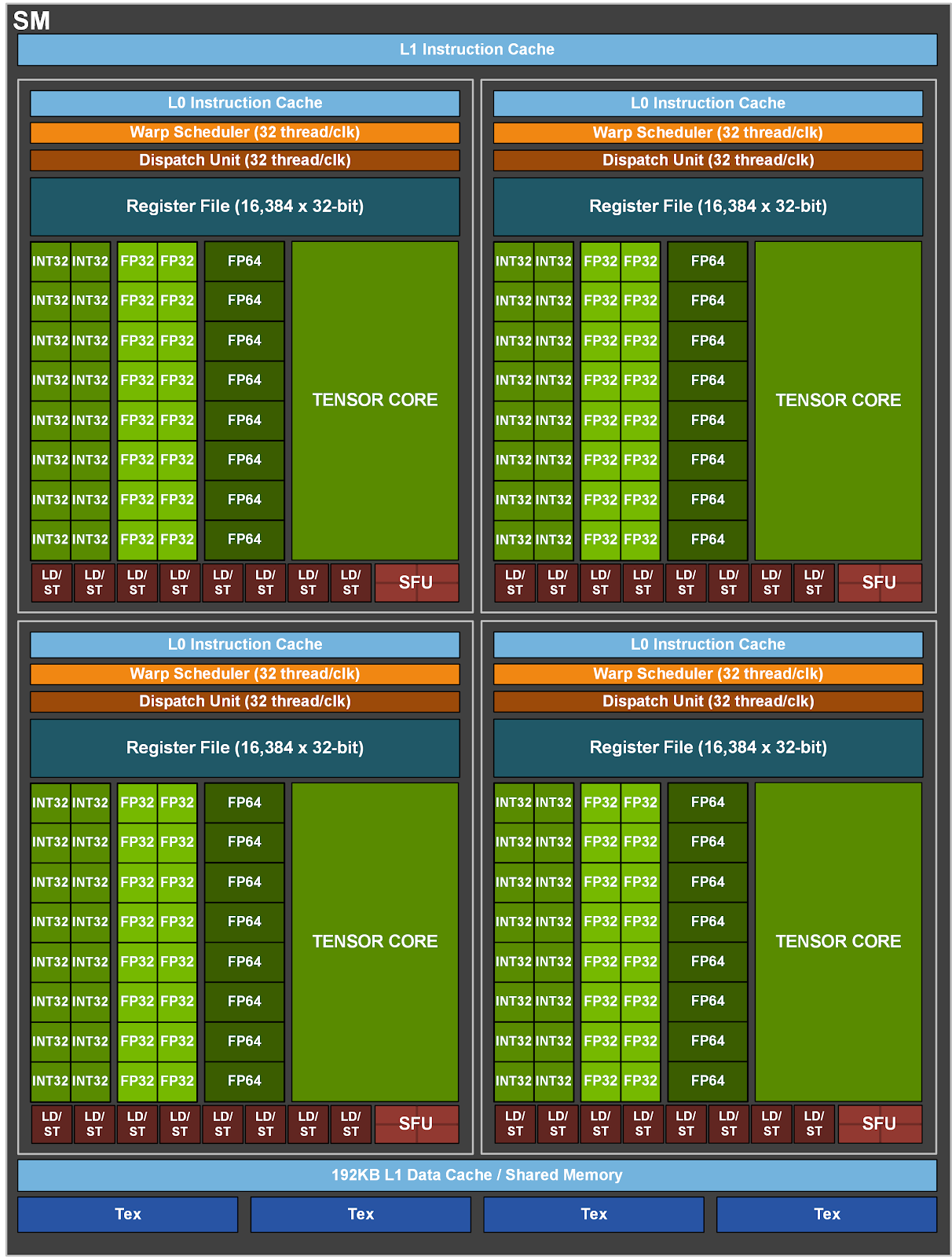
SM (Streaming Multiprocessors)
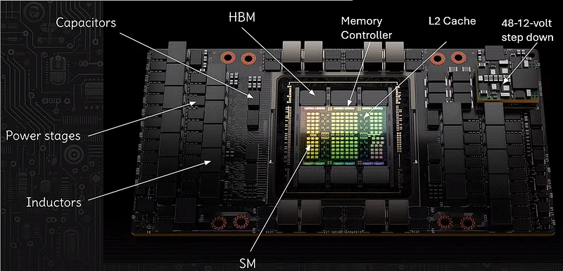
The SM, or Streaming Multiprocessor, is the fundamental building block of NVIDIA GPUs. Each SM contains CUDA cores (the processing units for general-purpose computing), Tensor Cores (specialized for AI workloads), and other components necessary for graphics and compute operations. SMs are highly parallel, allowing the GPU to perform many operations concurrently. In total, there are 144 Streaming Multiprocessors on the main die. But their parametric yield is around 90% which means we can use around 130 of those. Rest that fails during production is turned off. Also if you look at the size of the main die, that is quite a large die, and very close to the limitations of the modern-day fab machines. With the current system, we can’t make much bigger chips. And when we produce such chips, some multiprocessors are definitely going to fail.
If we talk about Google’s new TPU, they create much smaller chips and solve the networking separately.
HBM (High Bandwidth Memory)
HBM stands for High Bandwidth Memory, which is a type of stacked memory with high bandwidth interfaces. HBM provides significantly more bandwidth compared to traditional GDDR memory, allowing for much faster data transfer rates between the GPU and the memory, which is particularly beneficial for bandwidth-hungry tasks such as deep learning and big data analytics. If you look at the memory controller, you will see 6 of them, but NVIDIA only enables 5 of them.
Here’s an interesting bit, since the physical location of HBM’s are not equidistant to the SMs, a few SMs are faster and others are slower.
Memory Controller
The memory controller is an essential component that manages the flow of data between the GPU’s core and its memory (HBM). It coordinates read and write operations, addressing, and timing, ensuring that data is efficiently moved to and from the memory as required by compute operations.
L2 Cache
L2 cache on a GPU is a larger, slower type of cache memory compared to L1 cache. It stores frequently accessed data to reduce the time it takes to retrieve that data from the main memory. Having a large L2 cache can greatly improve performance by reducing memory latency and increasing data throughput. H100 is around 50 MB of cache.
Note: The rest of the components are just part of the power supply on the entire chip.
Capacitors
Capacitors on a GPU board serve as a temporary storage for electric charge. They help stabilize voltage and power supply by releasing charge when the voltage drops and absorbing excess charge when the voltage spikes. This smoothing of the electrical current is crucial for maintaining the stability and integrity of electrical signals within the GPU.
Power Stages
The power stages, also known as VRMs (Voltage Regulator Modules), are responsible for converting the voltage provided by the power supply to the lower levels that the GPU and memory chips can use. They are critical for providing clean and stable power to ensure the GPU operates efficiently and effectively.
Inductors
Inductors in the power supply circuit work alongside capacitors to filter out noise from the power supply. They store energy in a magnetic field when current flows through them and release it to smooth out the current flow, playing a vital role in managing the power delivery to the GPU.
48–12-volt step-down
This indicates a voltage step-down converter that transforms a higher voltage level (48 volts) to a lower level (12 volts) needed by the GPU. Efficient power conversion is crucial in high-performance GPUs to minimize energy loss as heat and ensure the delicate electronic components receive the correct operating voltage.
Actual power centers are providing power at a much higher voltage. But NVIDIA allows up to 48 volts, but the chip is operating on 12 volts.
Breakdown of the Chip
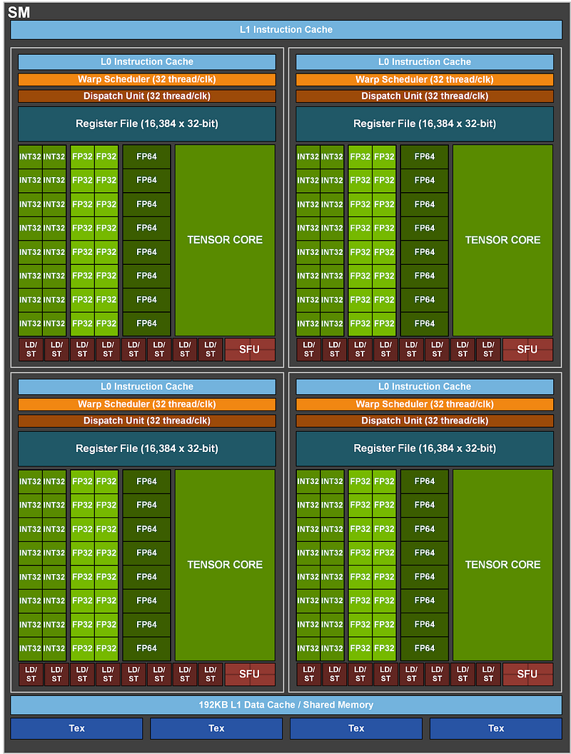
There are a lot of things happening in the SM, look at the Tensor core (the most important bit of the chip), which’s quite a big part of the SM. If we don’t use that tensor core we lose around 30x in terms of overall performance. This is where all the matrix multiplication are happening.
We have 256KB L1/shared memory, basically, this memory can be reconfigured by the programmer to act as L1 or shared memory.
Within each core, we see LD/ST (load and store), responsible for moving memory around. Then we have a lot of parallel units doing integer operations, floating point operations, etc.
We also have Warp schedulers that tell the chip where to execute the code in the chip.
We have Register Files, these are the fastest memory on the chip.
So, the way it is designed is to make everything as much parallel as possible. It has a fairly deep memory hierarchy, which enables the GPU to access the most important small information in the fastest way possible. However, the downside of this architecture is that it becomes increasingly tough to code things up in such a way that it efficiently uses memory.
The thing that we want to avoid as much as possible is writing up and down in the memory stack. Remember each memory level is of different speeds, and writing things across different types of memory is really expensive.
This is what Flash attention achieves, reducing the number of reads and writes.
H100 also has distributed shared memory which means we don’t need to write things to HBM and then make them available for the other SMs. With distributed shared memory different SMs can talk to each other without relying on the HBM.
To put things in perspective, HBM has a bandwidth of 3.35 TB/s, that’s unbelievably fast. L2 cache has a bandwidth of 12 TB/s. 33 TB/s for L1.
Here’s an interesting bit, if you run matrices that are smaller than 1000x1000, H100 is not going to be utilized properly. Now this might be a small thing for most of us, but can be crucial information when designing a hardware-aware algorithm.
So, how do we think about designing these systems?
When we think about things from a code perspective, we think of Time complexity and memory complexity.
But when we think of it from Chips’s perspective, it is about read/write in different layers of memory. We can have an order of magnitude faster results even with more operations if those are happening at a lower (faster) level of memory. This is what they achieved in Mamba as well.
Give a read to this, pretty interesting concepts there:
Systolic arrays
A systolic array is a grid of processors that rhythmically compute and pass data through the system. It’s used in computer architecture to perform matrix multiplication more efficiently, a key operation in deep learning and AI tasks. In NVIDIA’s H100 Tensor Core GPUs, systolic arrays are likely part of the Tensor Cores, which are optimized to accelerate AI workloads by performing dense matrix operations at high speeds. This allows for rapid and efficient handling of tasks like neural network training and inference.
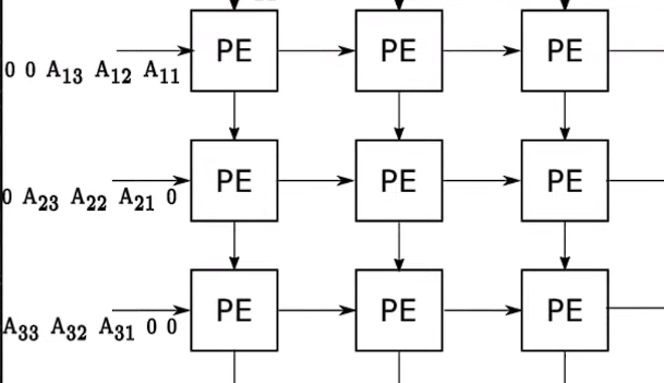
A systolic array differs from other compute units in how it processes data. In a typical processor, each compute cycle involves fetching data from memory, computing, and then writing results back to memory. This can create bottlenecks due to memory access times. In a systolic array, once data is loaded into the array, it’s passed from one processing element to the next in a coordinated fashion, often with each processor doing part of the computation. This “heartbeat” of data reduces memory reads and writes, allowing for many operations to be performed in each cycle, thereby increasing efficiency and speed, especially in matrix multiplication tasks.
Note: The modern AI hardware is usually not designed to keep the power requirements low, but it is primarily designed to be fast, as fast as possible.
There is so much I’ve not covered, we would need an entirely new blogging series that will explain how these chips are actually manufactured.
I’m not even a beginner in hardware design, but I wanted to take up something that I’ve never done before. It was extremely hard to write this piece up. Please support me by clapping and following.
Writing such articles is very time-consuming; show some love and respect by clapping and sharing the article. Happy learning ❤
Please don’t forget to subscribe to AIGuys Digest Newsletter


