
An Arduino Nano Electronic Speed Controller (ESC) — Part 2
In Part 1 we explained the design of our Arduino based ESC. Part 2 will focus on the power stage and why MOSFET drivers are needed. The most current that a digital pin from one of the Nano family can provide is 40mA and most of the boards have a capacity much less than this.
The BR2205 2300KV BLDC motors that we will be testing our ESC on have a maximum current draw of almost 30A. Hence the need for a power stage.

This series of articles was sponsered by PCBWay — PCB Prototype the Easy
Way! Thank you for providing all the prototype printed circuit boards used
in designing our Nano ESC carrier board.
5.0 The Power Stage (3-Phase Bridge)
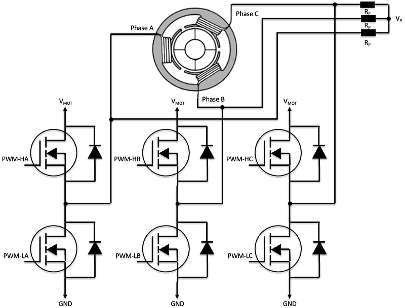
The motor power stage is a standard triple half-bridge setup, often used for 3-phase BLDC motors (Figure 1).
We will use MOSFET’s for the switches in our 3-phase bridge. The three main factors which drive MOSFET selection are:
1. Operating Voltage (motor supply is a 3S LiPo or up to 12.6 V) — choose a MOSFET whose drain-source voltage (VDS) is at least 20–50% higher than the motor supply voltage.
2. Maximum Current Draw (ID) — this will be determined by either the torque needed to start up the motor with a propeller fitted or the stall current. If you don’t want to use components that are rated to the stall torque, then you will have to monitor the current in each phase and shutdown the power stage if your limit is reached.
3. Power Dissipation (PTOT) — MOSFETs dissipate power and generate heat due to the drain-source resistance (RDS(ON)). Thermal constraints, including the ambient temperature and any heatsinking available for the MOSFETs, limits how much power can be dissipated. The maximum allowable power dissipation drives MOSFET selection based on the RDS(ON) value.
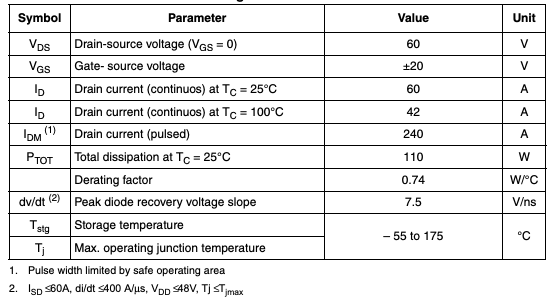
The MOSFET’s that we have selected as switches in the bridge are the STP60NF06, 60V N-channel Power MOSFET[1]. These FET’s have been designed for fast switching, and to minimize input capacitance and gate charge. The maximum ratings for this FET are shown in Figure 2.
Our FET can block up to 60V and handle up to 60A of current which is more than we need. The resistance when ON (RDS) is less than 0.016 Ω, so even at 30A the MOSFET will drop less than 0.5V across the drain and source. The typical gate charge (QG) is 54 nC at VGS = 10V, which is low compared to most power MOSFET’s (i.e., the STP60NF06 switches quickly). However, it will only switch fast if it can get enough current, which is why we normally use MOSFET drivers.
The threshold voltage (VTH) or gate-source voltage required to turn the MOSFET ON is 2–4V.
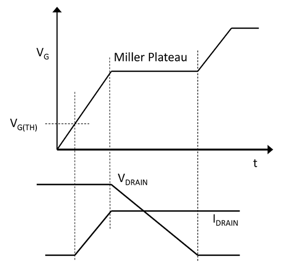
Miller Plateau

The Miller Plateau (Figure 3) in a FET is caused by the gate-drain
capacitance. Though smaller than gate-to-source capacitance, the
gate-to-drain capacitance goes through a voltage excursion that is
often more than 20 times that of the gate-to-source capacity[2].
Therefore, the gate-to-drain or Miller capacitance typically requires
more actual charge than the input capacitance.

If delivering a constant current into the gate, the voltage at the
gate is not a linear slope; it reaches a plateau during the time
that the MOSFET is switching. This is called the Miller Plateau.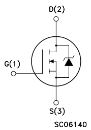
As shown in Figure 4, there is a body diode between the MOSFET source and drain. These diodes protect the MOSFET from the high voltage spikes that can occur when switching highly inductive loads like a motor. When the MOSFET switches OFF, the time it takes for the body diode to reverse direction is called the reverse recovery time (trr = 70 ns — see Figure 5).
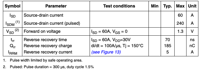
Diode Reverse Recovery Time

A diode which is forward biased will allow current to flow. Ideally,
when you switch voltage polarity across the diode and reverse bias it,
the diode will stop conducting immediately. In practise, there is a
finite amount of time before this happens which is called the reverse
recovery time (trr).

In other words, reverse recovery time is the amount of time current
flows in the reverse direction when the forward current switches
directions. This happens due to the residual stored charge in the diode.
6.0 MOSFET Drivers
Logic level MOSFET’s can be driven directly from an MCU pin. For larger power MOSFET circuits, there are four issues that make a direct connection problematic. They are:
- High gate capacitance — MCU output pins are designed to work with small capacitive loads (e.g., 10–100 pF). The STP60 has a gate input capacitance (CISS) = 1660 pF. This creates the current surge issue below.
- High Gate Voltage — often 3.3V or 5V is not enough to turn a power MOSFET hard ON, particularly for the high-side transistor. A MOSFET that is just ON will have a higher drain-source resistance and will dissipate more power as heat.
- Back Current — a switching MOSFET can cause current to flow from the gate to the MCU digital output pin. MCU IO current sink capability is less than they can source.
- Fast gate charge/discharge — We explained in the previous section that fast MOSFET switching is dependent on being able to deliver sufficient current to charge and discharge the gate.
MOSFET current is determined by the gate charge (QG) and how quickly you will be turning it ON and OFF. There is a design trade-off between low switching losses (which require fast rise and fall times) and low EMI (which requires slow rise and fall times). In addition, the pulse-width modulation (PWM) frequency and required duty cycle puts a time restriction on switching speed (e.g., a 20 kHz PWM frequency, with a 1% duty cycle requires a 500 ns pulse).
The current required may be calculated using:

For the STP60 MOSFET:
- Gate Charge (QG) = 54 nC (at VGS = 10V)
- Time to switch on/off (tswitch) = 500 ns (using above example)
- I = 54 nC / 500 ns = 108 mA
Ultimately, the switching performance of a MOSFET transistor is determined by how quickly the voltages can be changed across its effective terminal capacitance.
We can overcome the four issues listed above by using a MOSFET driver. These are designed to convert TTL level signals into high current outputs. Their high speed and current output enable them to drive large capacitive loads with high slew rates and low propagation delays. The high output current minimizes power losses in the power MOSFET by rapidly charging and discharging the gate capacitance.
The gate driver must be able to provide at least the amount of current needed to achieve the switching times described above, but a driver with more current capability can also be used.
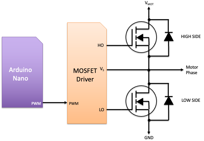
You can design the power stage with one driver per FET, but we will use an IC capable of driving two MOSFET’s in a half-bridge (Figure 6). We have a half-bridge driving each phase of the BLDC motor so we will need three of these IC’s and six MOSFET’s in total. We refer to the transistor connected to the positive motor supply as the high-side, and the one connected to GND (or negative power) as the low-side. A MOSFET driver that can provide switching current to a half-bridge is called a high-side/low-side driver.
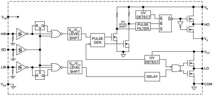
Based on our modest gate current requirements of around 100 mA, we have selected the IR2110PBF half-bridge gate driver (Figure 7). This model number is for the through-hole version, there is also a SMT version (IR2110S). The IR2110 is a high voltage, high speed power MOSFET driver with independent high-side and low-side referenced output channels. The IR2110 can handle gate currents up to 2A and is 3.3v — 5V logic compatible. The IRS2110 is the pin compatible replacement for the IR2110. Their block diagrams are identical.
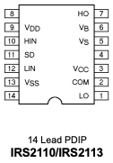
The IR2110 we are using has 14 pins but only 11 of them are used (Figure 8). The pin descriptions and purpose are as follows:
VDD — Logic Supply for the MCU controlling the IR2110. For the Arduino Nano this will be +5 VDC. When VDD = +5 V, the logic 1 input threshold of the IR2110 is slightly higher than 3V.
HIN & LIN — Logic inputs for high-side and low-side gate driver outputs (HO and LO), which are in phase. In other words, we connect the PWM signals from the MCU to HIN and LIN, while HO and LO are connected to the gates of the high-side and low-side MOSFET’s.
SD — Logic input for shutdown. If the SD pin is grounded, the driver is enabled. You can use this pin (ACTIVE HIGH) to disable the driver if required.
VSS — Logic ground for the MCU.
VCC — Low-side fixed supply voltage. This voltage is connected to the drain of the internal low-side MOSFET (Figure 7) and is recommended to be between 10 and 20 V [3].
VB & VS — High-side and low-side floating supplies.
COM — Low-side return for the gate driver (i.e., ground). While VSS and COM are not internally connected, the IR2110 is a non-isolated driver, meaning that VSS and COM should both be connected to ground.
When HIN is HIGH, HO turns the high-side MOSFET ON and when LIN is HIGH, LO turns the low-side MOSFET ON. The HO output is not with respect to ground, but with respect to VS. When HIGH, the voltage at HO is equal to VB, relative to VS. When LOW, the voltage at HO is equal to VS, relative to VS (i.e., zero).
The output on LO is with respect to ground. When LIN = HIGH, LO = VCC. When LIN = LOW, LO = VSS (GND).
HIN and LIN should never be HIGH at the same time or shoot through will occur, effectively shorting the motor supply voltage to GND.
The IR2110 includes undervoltage (UV) lockout on both channels (UV DETECT in Figure 7), which will turn OFF HO or LO if detected. This will trigger if VCC or VB gets below around 8.5V (somewhere between 7.0 and 9.7V, but typically 8.5V).
Coming Soon — Part 3 (The Bootstrap Capacitor)
The bootstrap capacitor is placed between the VB and VS terminals on the IR2110 (Figure 7). It is there to satisfy the requirements of driving the gate of the high-side MOSFET hard ON. Calculating the correct value for the MOSFET driver bootstrap capacitor is quite a mission!
If you enjoyed this article and would like to help support my writing, then please subscribe to become a Medium Member. I will get a portion of your subscription fee and you get full access to every story on Medium. Alternatively, you can buy me a coffee!
[1] Ref: https://www.jaycar.com.au/medias/sys_master/images/images/9729173127198/ZT2450-dataSheetMain.pdf
[2] Ref: https://www.infineon.com/dgdl/Infineon-Use_Gate_Charge_to_Design_the_Gate_Drive_Circuit_for_Power_MOSFETs_and_IGBTs-AN-v01_00-EN.pdf?fileId=5546d46267354aa001673ba630970081
[3] Ref: https://www.infineon.com/dgdl/Infineon-IRS2110-DataSheet-v01_00-EN.pdf?fileId=5546d462533600a40153567660ff27b0


