
An Arduino Nano Electronic Speed Controller (ESC) — Part 1
Now that we have delved into how BLDC motors operate and provided an overview of trapezoidal sensorless control, we can bring it all together in the design of an Arduino ESC shield. This exercise is a useful test of our understanding of the previous material.
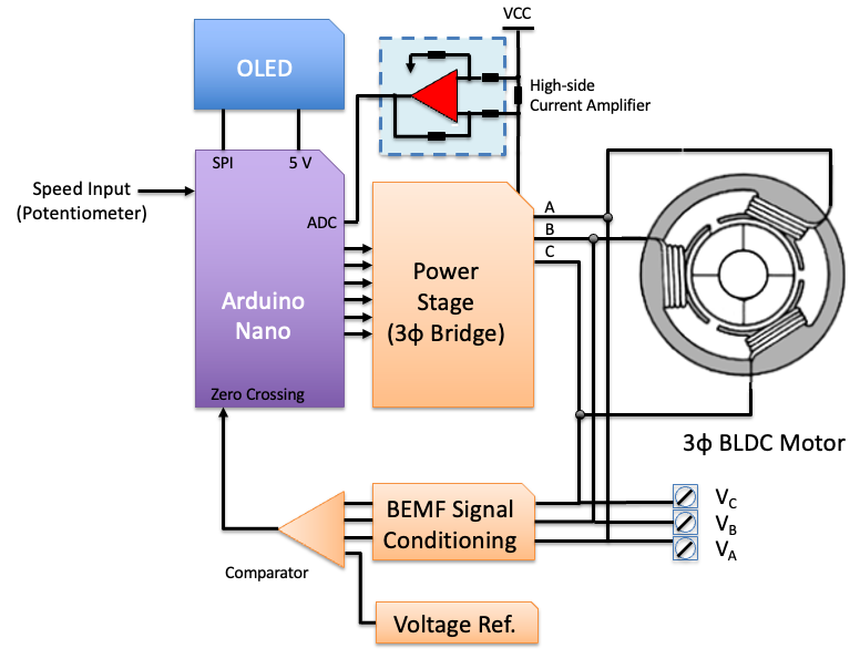
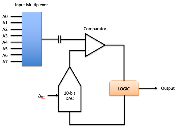
The block diagram for our ESC design is shown in Figure 1. We will use a board from the Arduino Nano family to orchestrate proceedings. Control of the motor speed will be by a PCB mounted potentiometer which will be converted to a PWM output. This design will allow us to test motors and map PWM duty cycle to BLDC motor RPM using an external tachometer.

This series of articles was sponsered by PCBWay — PCB Prototype the Easy Way! Thank you for providing all the prototype printed circuit boards used in designing our Nano ESC carrier board.We will break out the motor voltages to a terminal strip so that we can display the waveforms on an oscilloscope. The Arduino will also control an OLED display to provide feedback on the ESC status. Total motor current will be monitored using a high-side current amplifier and sense resistor.
Shield vs Carrier vs HATDifferent manufacturers use different names for PCB’s that add capability to their boards. The term shield is normally used to indicate an add on board which is plugged into the top of the Arduino pin headers. Devices from the Arduino MKR and Classic family can be easily “stacked” (Figure 157). Often the shield includes stacking headers, but users need to check that there is no pin conflict between multiple stacked shields. The hardware wont check for this.Normally the Arduino Nano family of boards don’t come supplied with stacking headers. In this case, the Nano is normally plugged into female headers on the extension board and this arrangement is called a carrier board.The Raspberry Pi term for a shield is a HAT (Hardware Attached on Top) for the model B+ or a pHAT (partial HAT) for the Zero form factor. In addition, to specifying pin specification and layout, HATs include the possibility of auto-configuration via an EEPROM which identifies the board and the IO pins used. Adafruit refers to pHAT’s as bonnets.The Arduino boards with the Nano pin layout and form factor are shown in Figure 2. To maximise compatibility between boards we will write the initial sketch to drive the carrier board using non processor specific code. If speed becomes an issue, we may need to move to register-based coding.
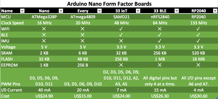
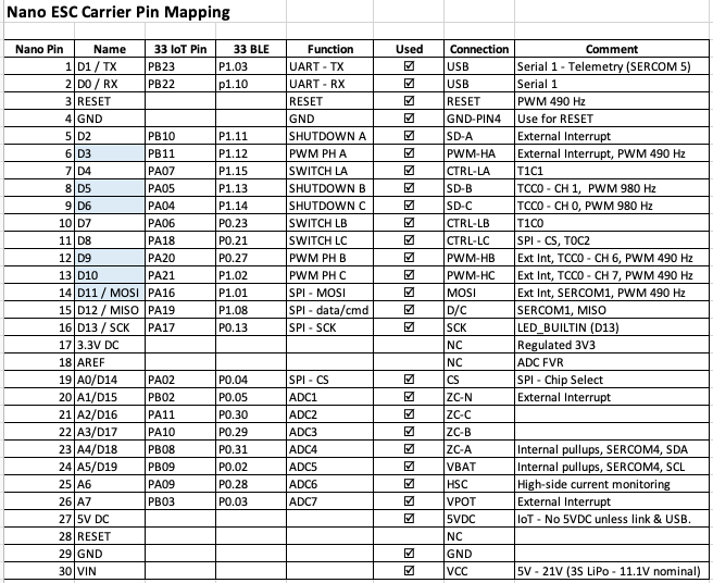
To keep track of what pins we have used on the Nano we use a pin mapping table (Figure 3). The pins that are highlighted in blue are capable of PWM. We needed three PWM pins with the same frequency (490 Hz). On the Nano, six of the analogue inputs can also be use as digital inputs/outputs.
In the following sections we will examine the design of the blocks shown in Figure 1, starting with the PWM duty cycle input selection (i.e., motor speed).
1. Manual Throttle
We want our carrier board to control the motor under test using a PWM signal generated by the Nano based on the position of the potentiometer (Figure 4).
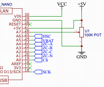
By passing a voltage through the potentiometer and connecting this to an analogue input on your Arduino (VPOT — A7), it is possible to measure the amount of resistance of the potentiometer because the two values are proportional (V = IR).
2. LiPo Battery Connection & Monitoring
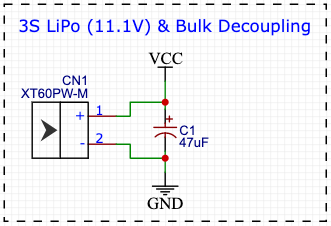
Motor power will be provided from a 3S LiPo battery. This will be connected using a male XT-60 socket on the PCB. A lot of hard to debug design issues come from the power supply and noise. The issue is that MCU current is drawn in very short spikes on the clock edges. If I/O lines are switching, the spikes will be even higher. If all eight I/O lines of an I/O port changes value simultaneously, the current pulses on the power supply lines can be several hundred mA. In addition, this is likely to happen when we are driving the motors which can create large current surges which result in the battery voltage sagging. The ATMega328P brown out detector will put the chip into reset mode if the voltage on the Vcc pin drops below a threshold. The brown-out detector (BOD) can be set for 1.8, 2.7 or 4.3V via the extended fuse byte. Arduino UNO’s are set at the 2.7V level, but as the 16MHz processor requires 3.78V so you are likely to see instability before the BOD is triggered. One solution to this “low frequency” ripple is to place a relatively large capacitor near the power supply. This is the purpose of C1 in Figure 5.
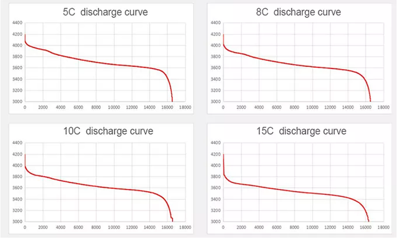
It is a bad idea to over discharge LiPo batteries, so we want to keep an eye on the battery voltage and stop the motors before it gets too low. The 3S battery we are using has a nominal voltage of 12 V and when fully charged, will put out 12.6 V. The characteristic curve for a 3S LiPo battery is shown in Figure 6. You don’t want to discharge the LiPo below 15% capacity (around 11.12 V), as it then quickly falls off the cliff and you can damage the battery.
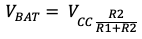
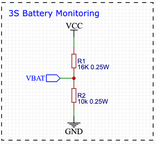
To monitor the battery, we will use a simple voltage divider and the ADC (Analog to Digital Converter) on the ATMega328P. We need the resistive divider because you can’t apply more than 5V to an Analog Input on the Nano. The circuit for a voltage divider is illustrated in Figure 7. Our LiPo has a maximum output of 12.6 V, and we can use the voltage divider formula below to work out R1 based on the recommended input impedance for the ADC being R2 = 10 kΩ, VCC = 12.6 V and VBAT = 5 V.
The ATMega328P has a 10-bit ADC. This means that it can return ²¹⁰ (i.e., 0–1023) values. The eight analogue inputs on the UNO are connected to the same ADC, so you can only sample 1 input at a time (Figure 8). The ADC Sample and Hold takes approximately 12μs, and the entire conversion process can take up to 260μs (depending on the pre-scaler selected). We will need to keep this in mind when we are polling the battery, motor current and manual throttle control potentiometer.
The ADC measures voltage by charging an internal 14pF capacitor and then measures that voltage with successive approximations. This implies that resistor R1 in our voltage divider (the input impedance) can’t be too large (> 70 kΩ) or the capacitor wont charge quickly enough.
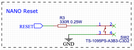
3. MCU Reset
The RESET pin on AVR devices is active-low and setting this pin low externally will reset the device. If an external switch is connected to the RESET pin, it is important to add a series resistance. Whenever the switch is pressed it will short the capacitor, and the current through the switch can have high peak values. This causes the switch to bounce and generate steep spikes in 2ms — 10ms periods until the capacitor is discharged. The PCB tracks and the switch metal introduces a small inductance and the high current through these tracks can generate component destroying voltages. Our design includes a series 330R resistor to prevent this (Figure 9).
4. OLED Display
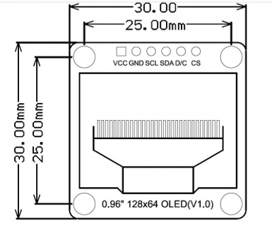
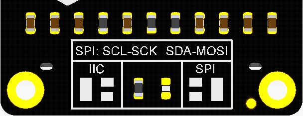
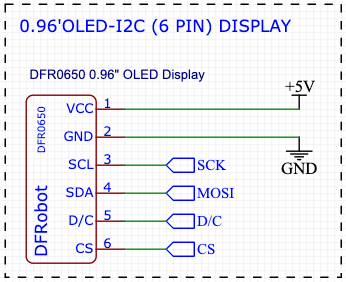
To indicate the current state of our Arduino ESC we will use a monochrome 0.96” OLED display from DFRobot called the DFR0650 (Figure 10). This module uses the SSD1306 driver chip, has 128 x 64 self-illuminating white pixels, and can communicate with the MCU using I2C or SPI. I2C is the default but we will use SPI because we need all the analogue inputs for the ADC. Frankly we would rather use I2C because it uses less pins and is simpler!
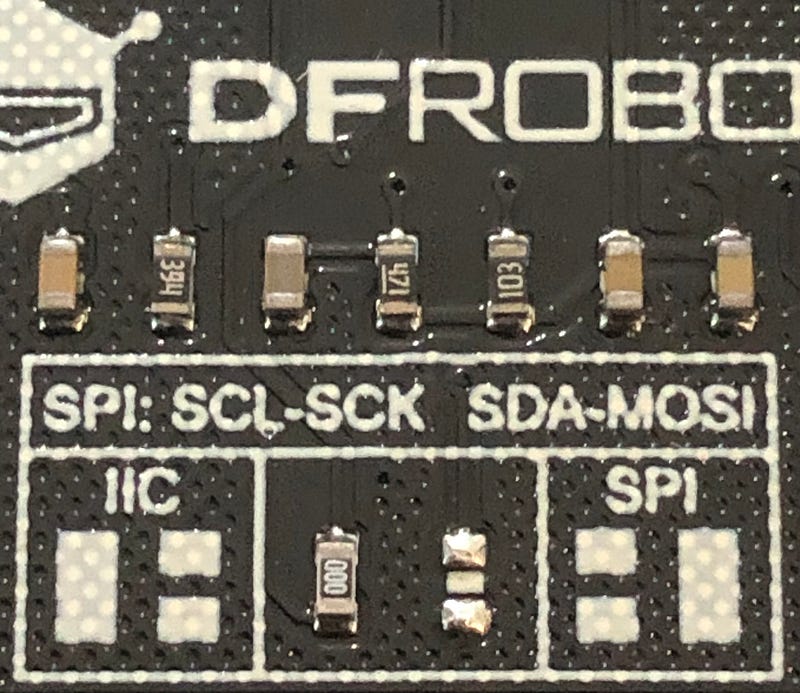
To enable SPI, you need to move the 0 Ω resistor located at the back of the PCB. The default position for this resistor (Figure 11) selects I2C communication. You need to de-solder the resistor and solder it to the adjacent pad (Figure 12).
The module can be powered from 5V or 3.3V and the I2C address is 0x3C. The SPI pin naming conventions can be a bit confusing. Normally, you need the clock pin (SCK), a data pin for the Arduino to send data (MOSI), a data pin for the Arduino to receive data (MISO), and a chip-select (CS) pin for each peripheral. However, the SPI standard is a bit fast and loose, meaning that some peripherals use the MOSI pin for receiving data and commands, and the data/command select pin (D/C) is set by the Arduino to indicate what it is being sent. To make things more confusing, MISO has recently been renamed CIPO (Controller In, Peripheral Out) and MOSI is now COPI (Controller Out, Peripheral In).
To operate the display using SPI, we need to connect 6 pins, VCC (5 V), GND, MOSI (D11), D/C (D9), SCK (D13) and CS (D10) — refer to Figure 13. With all the LEDs ON, the module draws approximately 24 mA. The Nano uses the LM1117IMPX-5.0 low drop out linear regulator to provide 5V. This can provide up to 800 mA, so we have plenty of capacity.
Coming Soon — Part 2 (The Power Stage)
In Part 2 of this series we will design the power stage used to drive our 3-phase Brushless DC (BLDC) Motor. We need this because digital outputs on the Nano can source at most 40 mA and our motor could draw over 30 A.
If you enjoyed this article and would like to help support my writing, then please subscribe to become a Medium Member. I will get a portion of your subscription fee and you get full access to every story on Medium. Alternatively, you can buy me a coffee!
[1] Ref: https://wiki.dfrobot.com/Monochrome_0.96_128x64_IIC_SPI_OLED_Display_SKU_DFR0650


