
美國硬體工程師必勝面經
硬體面試會遇到的 4 大主題 — RTL、Cache、CPU、Transistors

前言
在美國的留學生,頂著唸書的壓力又要找工作,讓人身心俱疲。被美國研究所的龐大的作業、實驗積滿了時間; 對於找工作的變數感到恐慌; 巨大的金錢壓力讓你喘不過氣。身為過來人,我了解到硬體相關資源的稀少,因此我想分享當時準備硬體工程師的面試題目,藉由本文讓疲於準備課業的硬體學生們,快速熟悉面試題目。
除此之外,對於本人找工作的經驗,可以參考下篇文章:
一、硬體程式問題
*程式碼的參考解答都可以在這邊找到:EDA Playground
# 基礎 RTL 語法問題如下:
- wire 類別跟 reg 類別的不同 ➡ wire 不能存資料,就像一線,reg 則可以存資料
- if else/case 語法在合成過程中會變成什麼 ➡ Multiplexer
- 如何避免 Inferred Latches — 確保所有條件分支的所有條件都有提供結果,或者有提供 Default Condition
- a = #5 b 跟 #5 a = b 的差別 前者:先判斷 b 的值,並存到暫存器中,過了 5 單位時間在賦值給 a 後者:有點像是 Gate Delay,過 5 單位時間在將 b 賦值給 a
# RTL 程式問題
- Design FIFO Buffer ➡ 參考連結內 fifo.sv 幾乎算是必考題,我遇過兩次不同公司的面試都有遇到。因此可以試著自己寫一個 FIFO,並嘗試解釋自己的程式碼。
- Design a generator that given 8 bits vector if the LSB bit is one, then the output should be 1 at that bit and the rest is 0 ➡ 參考連結內 generator.sv 這是一個 Priority bit vector 的題目,譬如說 input 是 b’00011010 那 output 就是 b’00000010。你可以用硬解的方法,然後面試者會請你該如何優化面積以及 Critial path。。
# 進階 RTL 程式問題
- Design Linked-List Buffer ➡ 參考連結內 linked_list.sv 直接開一個 Memory 而其 Address 可當作值以及下個節點的位置,這樣就可以避開 Pointer 讓解法更簡單。
- Design LRU Controller ➡ 參考連結內 LRU.sv 這是我遇過最難的一個程式題,最後只解到一半,提供在連結,也是不要去想 Pointer,而去利用硬體的思路解。
二、快取記憶體 — Cache
# 介紹 3C Models (與 Miss rate 有關)
- Compulsory Miss ➡ Item has never been in the cache since the program just started. Instruction Prefetch or Instruction Parallelism can improve it.
- Capacity Miss ➡ Item has been in the cache, but space was tight and it was forced out. Larger cache size can improve it
- Conflict Miss ➡ Item was in the cache, but the cache was not associative enough, so it was forced out. Higher Associativity and better Cache Replacement Policy (e.g. LRU) can improve it
# 優化快取效能 Cache Optimization
根據以下平均存取記憶體時間公式,因此如果能降低 3C,cache miss rate 就會降低,提升存取記憶體的時間,但同時會有一些 Trade-off。
Average Memory Access Time (AMAT) = Hit Time * (1 - Miss Rate) + Miss Penalty * Miss Rate
以下是利用不同技巧來降低 Hit time (HT)、Miss Rate (MR) 以及 Miss Penalty (MP) 的方法,可以好好研讀,面試會考之間的 Trade-off,如在不同的環境下,如何選擇可以最大化效能,而忽略掉 Trade-off。
- 如當程式碼有 Spatial Locality,Larger Block Size 是個好選擇,儘管他會增加 Miss Penalty。
- 又或者當程式有 Time Locality 的話,或許 Higher Associativity 有幫助 Keep often-used data in the cache 來降低 Miss rate。
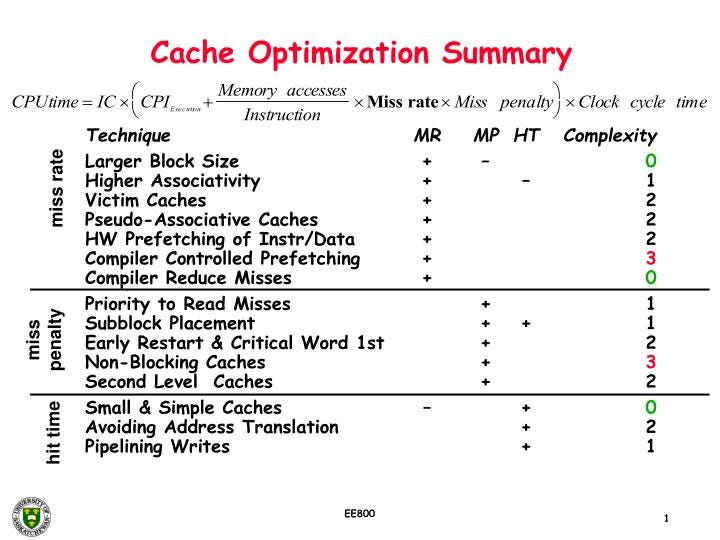
常問問題:
Q: How to optimize cache?
A:
1. Reduce hit time → small size and lower associativity, way prediction
2. Increase Cache BW → Multi-Banked Cache, power could be small
3. Reduce Miss Penalty → large cache block, critical word first, early restart, cache blocking
4. Reduce Miss Penalty or Miss rate → hardware prefetch
# 快取一致性 Cache Coherency
- MSI/MESI Protocol 是如何運作的,通常會出情境題: 給一系列的 Read/Write cache lines 過程,問某一個 cache line 的 state會如何轉換; 以及暸解 MSI → MESI → MOESI 的進化過程
- MESI 比 MSI 更 Efficient: 因為當 cache line 在 Exclusive state 時Write 不需要 broadcast 到其他 cache 去 invalidate。
- 而 MOESI 比 MESI 更好的原因: 當 cache line 在 Owned state 時,不需要 Write back to memory 就能 share cache data。
隨手筆記:
MSI - broadcast miss on bus to invalidate shared cache
MESI - if the line is not shared and clean, it is in exclusive state, and won't broadcast invalidate signal when write to the line → work well on multi-program applications
MOSEI - it allows sending dirty cache line directly between caches instead of writing back to a shared outer cache and then reading from there

常問問題:
Q: Why would we choose MOESI over MESI? Do many loads favor MESI or MOESI? Do many
stores many MESI or MOESI?
A: MOESI has the advantage that one cache can write a line and still allow other caches to be in
the shared state. With MESI, each write would invalidate the line in all other caches that would
cause future cache misses. Many loads favor MOESI. Many stores favor MESI the owned state
causes a broadcast for each store.
三、計算機架構 — Computer Architecture
# 5 階層管線化處理器 5-Stage Pipelined CPU
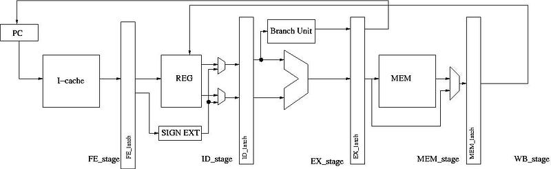
了解 IF/ID/EXE/MEM/WB 每個階層各在做什麼
- IF ➡ Fetch from instruction cache
- ID ➡ Decode instruction, immediate, get register value
- EXE ➡ ALU operation
- MEM ➡ Write results to memory
- WB ➡ Write results back to reg file
# 亂序處理器 Out of Order Processor
了解 Tomasulo’s Algorithm。當面試官給出一串指令,能說出以下三個步驟會如何跑
三個步驟
- In-order Issue — If reservation station free, issue instr & send operands to the reservation station. This steps also performs the process of renaming registers
* Reservation
負責儲存要被執行的指令 (Instruction),當 Registers 都準備好後就會執行指令。
* Registers Renaming
達到 Out-of-order 的原因,解決 Data Dependencies 的問題。- Out-of Execution — When operands ready, execute. If not, watch CDB (Common Data Bus) for results
- Write Result — Broadcast to register file and other reservation stations
Hardware Speculation — Reorder Buffer (ROB)
利用一個 ROB 儲存指令執行後的結果,多了一個 Commit 階段。因此在做 Instruction Speculation 時,結果不會馬上 Commit,而是存在 ROB 裡,等到真正確認 Branch 結果時才 Commit。
危障 Hazards
了解 Hazards 的發生條件以及解決方式。如給你一連串的 Read/Write sequences, 會發生如何的 Hazards 跟解決方式。
- Data Hazard — 當 Read/Write 同個 Data 時會遇到,OoO 透過 Register renaming 及 Reservation Center 解決。
Read-after Write (RAW) - Data dependencies,Register Renaming
Write-after Read (WAR) - name dependencies,Reservation Station 會 Buffer 要 Read 的資料
Write-after Write (WAW) - name dependencies,一樣可以靠 Reservation Station Buffer 要寫入 Register File 的結果。
- Control Hazard — 例如遇到 Branching,該 Take 哪方?ROB 跟 Pipeline flush 都是解決 Control Hazard 的方法。
- Structural Hazard — Lack of memory/computing resources,解法很單純,就是放多一點 Memory 或者計算單元。
虛擬地址翻譯 Virtual Address Translation
- CPU Request Virtual Address
利用 Page Table Register 或者 TLB (Cached 的 Page Number) 翻譯虛擬 Page Number 成實體 Page Number,如下圖:

- Calculate Page Table Register
假設你的 virtual address 32 bits, page size = 4k (10 bits),總 total 有 2²⁰ 個 Pages,每個 page 4 bytes → Page Table Register 大小為 4MB
- 提升翻譯速度的方法 (Increase Hit Time)
Translation Look-aside Buffer (TLB): 暫存常用的 Page Number,讓翻譯速度更快 → Increase Hit Time
Virtually Indexed Physically Tagged Cache: 在翻譯 Page Number (Upper part) 的時候,利用 Lower part of the address 去存取 Cache,讓兩件事能平行處理。
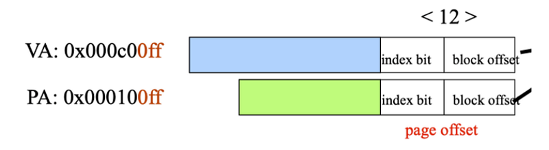
使用 VIPT 要能達成以下條件,因此對於 Cache size 會有要求。
Index Bits + Block Offset Bits == Page Offset Bits
常問問題:
Q: What's the maximum size for a 4-byte block direct-map cache if we want to virtually indexed physically tagged cache?
A: Page Size 為 4k (12 bits),4-byte block (2 bits),因此 index bits 只能 10 bits。
對於一個 direct-map cache 就代表有 2^10 個 entries,因此最大的 cache size 為 2^10 * 4 bytes = 4kB
四、電晶體問題
邏輯問題
# Universal Gates
NOT → sel → A, i0 → 1, i1 → 0
AND → sel → A, i1 → B, i0 → 0
OR → sel → A, i1 → B, i0 → 1
# Dynamic Logics
如 Domino Logics,了解他的運作模式
1. Pre-charge - Using clock signal so that the PMOS could be strong
2. Evalution - Put an inverter to prevent the next gate from discharging.
For example, when input A transit from 1 → 0, if there's delay, Y could drop a little bit
from Vdd.
優化關鍵路徑 Critical Path
常問如果你不能調整時脈,該如何優化 Critial Path?
- 使用面積較小的電晶體。
- 邏輯管線化 (Pipeline),中間放 Registers。
- 將一個複雜的單元,更模組化,一些 Tools 才比較好去優化電路。
面積、速度、功耗 — Area, Timing, Power
P = CV²f 這個就會是相當重要的公式
電晶體變小 → 面積變小 → 在相同功耗下,時脈可以變快
而在 Power 上也會細問如 :
- Static Power — 電晶體沒在工作時的電耗,原因為 sub-threshold current, gate leakage, body effect,又稱 Short-Circuit Power
- Dynamic Power — 電晶體充放電的結果,又稱 Switching Power
而達到 Low Power Design 可以利用以下三個方法:
- Clock Gating — 把 Clock 擋住,不讓電路充放電,降低 Dynamic Power
- Power Gating — 直接把電路關掉,連 Static Power 都消除
- Multi Voltage — 讓不同的電路有不同的工作電壓,讓能接受慢速的電路擁有較低的工作電壓。
佈局
# CTS (Clock Tree Synthesis) —藉由塞 buffers 解決 Clock Skew 的問題,來確保 clock 能平均的傳到晶片的各個角落。
# Wire Crosstalk — How to order the wire sequence with signals A, A bar, and B where B is the critical signal
# How to resolve congestion
這個比較偏一些使用 Physical Design 軟體工具的實作技巧
- Adjust the position of the IP
- Add false path, preventing tool to do unnecessary optimization to reduce buffer
- Utilize Blockage at the macro cell
結語
以上為一些常見的硬體工程師面試題目,從數位設計到佈局工程師都會蠻受用的,沒辦法全部都能涵蓋到,但是希望能給予有背景的讀者一些 Hint,知道準備的方向。搭配一些課堂素材以及 Google,就能輕鬆破解面試!
參考
個人面試 Apple、Nvidia 及一些硬體新創的經驗