
Investment Chances — New Export Controls on Semiconductor Technologies to China
On 12th August 2022, the U.S. Department of Bureau of Industry and Security (BIS) announced that it would cut off the supply of Electronic Computer-Aided Design (ECAD) software specially designed for the development of integrated circuits with Gate-All Around Field-Effect Transistor (GAAFET), two substrates of ultra-wide bandgap semiconductor (Gallium Oxide, Ga2O3), and diamonds, and Pressure Gain Combustion (PGC) technology.
1st — (17th April 2018) Ban American firms selling components to the Chinese telecom equipment maker ZTE corporation 2nd — (16th May 2019) — Ban Huawei from buying components from U.S. companies without government approval 3rd — (12nd August 2022) — Cut off the supply of ECAD, ultra-wide bandgap semiconductor, and pressure gain combustion technology to the entire Chinese enterprise
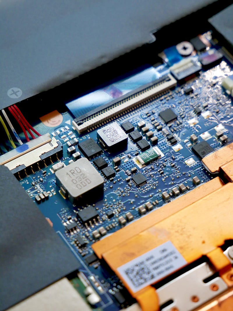
In semiconductor manufacturing, the 3nm process is the next die shrink after than 5nm MOSFET (Metal-Oxide-Semiconductor field-effect transistor) technology node. The semiconductor process has entered the post-3nm process, Moore’s Law is not applicable to a certain extent, and the semiconductor industry is adopting a new all-gate field effect transistor (GAAFET) to deal with more advanced processes to replace the Fin Field-effect transistors that have been used before.
3nm Process 1.TSMC (taiwan) — FinFET (Fin Field-effect transistor) 2. Samsung Electronic (Korea) — GAAFET (Gate-all-around field-effect transistor)/MBCFET (Multi-bridge channel field-effect transistor) 3. Intel
This embargo is related to the pattern of semiconductors in the next decades. The embargo of the U.S. Department of Bureau of Industry and Security (BIS) is not all EDA software, but it is the EDA software modules designed for an emerging technology called gate-all-around (GAAFET) chips. In other words, this is a ban on the sale of advanced modules for advanced processes.
The Restriction 1. The United States has banned ASML (Netherlands) from selling Extreme ultraviolet lithography (EUV) machines to China 2. The United States is considering to ban ASML (Netherlands) from selling Deep Ultraviolet (DUV) lithography machines that can process more than 128 layers of flash memory 3. Kelei Semiconductor (KLA-Tencor) and Lam Research Corporation have announced that they will no longer sell 14-nanometer equipment to China.
The Concept of EDA technology
It is the concept of computational modeling, computational thinking, and computational exploration in the field of electronic circuit design engineering. It has changed the way electronic engineers design and manufactures integrated circuits. EDA technology is the result of an interdisciplinary collaboration between computer science and engineering. Now, designing any electronic circuit goes through a series of synthesis, conversion, optimization, digital simulation and prototyping, verification, and finally fabrication through advanced lithography and chemical process.
1. Computer scientists, electrical engineers, and EDA product engineers design and develop circuit models at different levels. 2. EDA product engineers work with physicists and chemists to develop manufacturing models. 3. They work with computer scientists to perform various complexity analyses. 4. They work with applied mathematicans to develop simulation and synthesis algorithms that scale well 5. They work with application domain eperts to develop intellectual property (IP) libraries
EDA Software Companies
- Agnisys
- Aldec
- Altair Engineering
- Altium
- Ansys
- Arteris
- Autodesk
- Cadence Design systems
- COSEDA Technologies
- Dassault Systems
- Dolphine Design
- EasyEDA
- EasyLogix
- Eremex
- IC Manage
- Ing-Buro FRIEDRICH
- JEDA Technologies
- Keysight Technologies
- Lauterbach
- Siemens EDA (Mentor Graphics)
- VisualSim Architect
- National Instruments
- Novarm
- Silvaco
- Synopsys
- WestDev
- Zuken
- Lattice Semiconductor
- Intel
- Microsemi
- Xilinx
- Digi-key
- RS component
- gEDA
- KiCAD
The Semiconductor Ecosystem
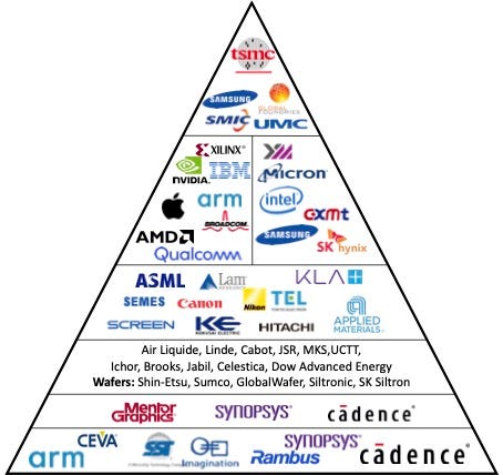
The rapid development of the semiconductor industry is bound to the EDA software. The function of the EDA software is to perform layout, routing, and pre-analysis in the small space of the chipset. Without EDA software, the cost of the design and manufacture of semiconductors is very high. The continuous development of EDA has successfully smoothed out the possible skyrocketing design costs. According to the analysis of Andrew B. Kahng of the University of California, the design cost of a system-on-chip (SoC) in 2011 was about $40 million compared to $7.7 billion without EDA software. It can be seen that the EDA software reduces the design cost by about 200 times.
However, the rapid development of China’s semiconductors changed the industry structure. For example, Primarius Technologies and Huada Jiutian are famous EDA corporations. However, the China EDA software corporations may not be able to challenge the top 3 foreign EDA software corporations. The top 3 chipset design software companies have always regarded China as an important customer. For example, 13% of Cadence’s revenue came from China, and 17% of Synopsys’s revenue came from China. However, China seldom invests in the advanced process of GaaFET. The supply restriction on the functional modules of EDA software to china has little impact on the EDA software corporation’s income, but it has a huge technological impact on China’s semiconductor development.
The U.S. actions appear to be more aggressive to block Chinese semiconductor technology outside the 14-nanometer wall. Now, China has to solve the supply of lithography equipment and advanced process of EDA software, so that China’s semiconductors will not lose to any developed countries. However, the EDA software is very hard for China to catch up with.
The top 3 EDA corporations might get even more competitive advantages when China is blocked outside the 14-nanometer wall.
References
https://min.news/en/economy/a85be8c0062cd6e6f0084ef8ce1fa98a.html
If you’ve found any of my articles helpful or useful then please consider throwing a coffee my way to help support my work or give me patronage😊, by using
Last but not least, if you are not a Medium Member yet and plan to become one, I kindly ask you to do so using the following link. I will receive a portion of your membership fee at no additional cost to you.


